TTL buffer
7400
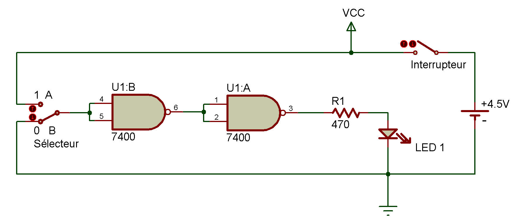
Ever wonder what happens when you start adding digital circuits together, using the output of one as the input of another?
Build this Project and find out. You can see from the schematic that we take the output from one NAND gate and use is as the input of another, You can see from the schematic that we "split" the output of the first NAND and use it for the inputs to the second (so that the two inputs for the second NAND will be the same).
From what you know about NANDs, what do you think will happen if the input to the first NAND is 1?
If the first input is 0?
Try to figure it out before building this Project. As you make the wiring connect ions, set the Select Switch to B. Switch power ON. What does LED 1 do?
Now set the Select Switch to A. LED 1 lights up.
As you've probably figured out, 1 is the input when the Select Switch is set to A, with an input of 0 coming when the Select Switch is at B.
What happens is that if the input to the First NAXD is 1, its output is 0. But the 0 output of die first NAND is the input of the second.
The 0 input to the second causes its output to become 1, lighting the LED. Sometimes we use buffer circuits to simply keep two portions of a device isolated from each other. This type of circuit does that job well.

![]()